自己参考mcbtms570评估板(主芯片为TMS570LS20216)做的板子(主芯片为TMS570LS3137)。
当前状态:
1. 所有供电和时钟都正常;
2. XDS100V2的固件正常,使用xds100serial工具检测仿真器正常;
3.TMS, TDI, TDO,TCK, RTCK, XDS_JTAG_RESET, XDS_JTAG_TRST与评估板设计一致;
4. TMS570的NERROR信号为高。
遇到的问题:
使用CCS6.2建立工程,进行仿真器连接测试时,TMS, TDI, TCK, RTCK, XDS_JTAG_RESET, XDS_JTAG_TRST的信号与评估板一致,但与TMS570连接的TDO一直为低电平。
而使用评估板连接正常。
ccs6.2仿真器连接测试结果如下:
[Start]
Execute the command:
%ccs_base%/common/uscif/dbgjtag -f %boarddatafile% -rv -o -F inform,logfile=yes -S pathlength -S integrity
[Result]
-----[Print the board config pathname(s)]------------------------------------/root/.TI/1524211065/0/0/BrdDat/testBoard.dat
-----[Print the reset-command software log-file]-----------------------------
This utility has selected a 100- or 510-class product.
This utility will load the adapter 'libjioserdesusb.so'.
The library build date was 'DEC 6 2017'.
The library build time was '00:19:23'.
The library package version is '5.1.232.0'.
The library component version is '35.34.40.0'.
The controller does not use a programmable FPGA.
The controller has a version number of '4' (0x00000004).
The controller has an insertion length of '0' (0x00000000).
This utility will attempt to reset the controller.
This utility has successfully reset the controller.-----[Print the reset-command hardware log-file]-----------------------------
The scan-path will be reset by toggling the JTAG TRST signal.
The controller is the FTDI FT2232 with USB interface.
The link from controller to target is direct (without cable).
The software is configured for FTDI FT2232 features.
The controller cannot monitor the value on the EMU[0] pin.
The controller cannot monitor the value on the EMU[1] pin.
The controller cannot control the timing on output pins.
The controller cannot control the timing on input pins.
The scan-path link-delay has been set to exactly '0' (0x0000).-----[The log-file for the JTAG TCLK output generated from the PLL]----------
There is no hardware for programming the JTAG TCLK frequency.
-----[Measure the source and frequency of the final JTAG TCLKR input]--------
There is no hardware for measuring the JTAG TCLK frequency.
-----[Perform the standard path-length test on the JTAG IR and DR]-----------
This path-length test uses blocks of 64 32-bit words.
The test for the JTAG IR instruction path-length failed.
The JTAG IR instruction scan-path is stuck-at-zero.The test for the JTAG DR bypass path-length failed.
The JTAG DR bypass scan-path is stuck-at-zero.-----[Perform the Integrity scan-test on the JTAG IR]------------------------
This test will use blocks of 64 32-bit words.
This test will be applied just once.Do a test using 0xFFFFFFFF.
Test 1 Word 0: scanned out 0xFFFFFFFF and scanned in 0x00000000.
Test 1 Word 1: scanned out 0xFFFFFFFF and scanned in 0x00000000.
Test 1 Word 2: scanned out 0xFFFFFFFF and scanned in 0x00000000.
Test 1 Word 3: scanned out 0xFFFFFFFF and scanned in 0x00000000.
Test 1 Word 4: scanned out 0xFFFFFFFF and scanned in 0x00000000.
Test 1 Word 5: scanned out 0xFFFFFFFF and scanned in 0x00000000.
Test 1 Word 6: scanned out 0xFFFFFFFF and scanned in 0x00000000.
Test 1 Word 7: scanned out 0xFFFFFFFF and scanned in 0x00000000.
The details of the first 8 errors have been provided.
The utility will now report only the count of failed tests.
Scan tests: 1, skipped: 0, failed: 1
Do a test using 0x00000000.
Scan tests: 2, skipped: 0, failed: 1
Do a test using 0xFE03E0E2.
Scan tests: 3, skipped: 0, failed: 2
Do a test using 0x01FC1F1D.
Scan tests: 4, skipped: 0, failed: 3
Do a test using 0x5533CCAA.
Scan tests: 5, skipped: 0, failed: 4
Do a test using 0xAACC3355.
Scan tests: 6, skipped: 0, failed: 5
Some of the values were corrupted - 83.3 percent.The JTAG IR Integrity scan-test has failed.
-----[Perform the Integrity scan-test on the JTAG DR]------------------------
This test will use blocks of 64 32-bit words.
This test will be applied just once.Do a test using 0xFFFFFFFF.
Test 1 Word 0: scanned out 0xFFFFFFFF and scanned in 0x00000000.
Test 1 Word 1: scanned out 0xFFFFFFFF and scanned in 0x00000000.
Test 1 Word 2: scanned out 0xFFFFFFFF and scanned in 0x00000000.
Test 1 Word 3: scanned out 0xFFFFFFFF and scanned in 0x00000000.
Test 1 Word 4: scanned out 0xFFFFFFFF and scanned in 0x00000000.
Test 1 Word 5: scanned out 0xFFFFFFFF and scanned in 0x00000000.
Test 1 Word 6: scanned out 0xFFFFFFFF and scanned in 0x00000000.
Test 1 Word 7: scanned out 0xFFFFFFFF and scanned in 0x00000000.
The details of the first 8 errors have been provided.
The utility will now report only the count of failed tests.
Scan tests: 1, skipped: 0, failed: 1
Do a test using 0x00000000.
Scan tests: 2, skipped: 0, failed: 1
Do a test using 0xFE03E0E2.
Scan tests: 3, skipped: 0, failed: 2
Do a test using 0x01FC1F1D.
Scan tests: 4, skipped: 0, failed: 3
Do a test using 0x5533CCAA.
Scan tests: 5, skipped: 0, failed: 4
Do a test using 0xAACC3355.
Scan tests: 6, skipped: 0, failed: 5
Some of the values were corrupted - 83.3 percent.The JTAG DR Integrity scan-test has failed.
[End]
想要得到的帮助:
1. 请问此错误可能的原因是什么?(因为在同一软件环境,评估板正常,但自己的板子报错,所以推测是硬件问题,但是JTAG处的电路设计与评估板完全一致,除TDO管脚外,其他JTAG信号用示波器测试都正常)
2. 如何隔离问题,究竟是仿真器端的问题,还是TMS570没有正常工作?
3.如何验证TMS570是否已经正常工作?在无法烧入程序的前提下,如何判断TMS570的工作状态?
请论坛的各位大神指点指点。
↧
XDS100V2与TMS570LS3137通讯异常
↧
TMS570LS0714的PWM波产生trigger开始ADC采样问题
如题,在使用PWM波产生AD采样的事件时,不能使AD采样。
我已经设置是AD采样换成硬件触发,PWM的SOCA使能,并且在软件触发下AD采样能够正确采样。
现在的问题是我怎么知道自己PWM波确实产生了事件,如果产生了事件为什么触发不了AD采样呢?
谢谢!
↧
↧
F021 API 擦除Flash总是在while(FAPI_GET_FSM_STATUS!=Fapi_Status_Success);这里死住;
使用官方给 的Bootloader uart 的程序在下载的时候总是 在
Fapi_issueAsyncCommandWithAddress(Fapi_EraseSector, eraseStartAddr);
while( FAPI_CHECK_FSM_READY_BUSY == Fapi_Status_FsmBusy );
之后 死在这一句----》while(FAPI_GET_FSM_STATUS != Fapi_Status_Success);
不知道为什么,希望大家能给我解答一下,官方的更好;
↧
RM46L852
RM46L852的定时器初始化代码怎么生成?使用HET_IDE软件?
↧
RM46L852
请问RM46L852的定时器怎么初始化?我现在需要一个定时器,每1ms中断一次
↧
↧
在使用F021 Flash API时如何将flash程序搬到RAM
您好!
我在使用官方的TMS570LS1224的LaunchPad时,使用官方提供的F021 Flash API 对内置的flash进行操作,在Fapi_setActiveFlashBank( Fapi_FlashBank0) 时,会出现错误异常,进入undefEntry 状态。 然后将Fapi_FlashBank0 改为Fapi_FlashBank7 程序就完好,并且擦写都正确。
我想问: 1. 是不是因为程序存储在Flash Bank 0 中,所以使用API 不能对BANK0进行操作?
2. 如果要对Bank0进行擦写操作,有什么办法? 需要将Flash API程序 弄到RAM中,然后在RAM中执行flash API 对 BANK0 进行擦写操作?
3. 问下如何才能将FLASH API 或程序 弄到RAM中进行操作,有没有相关例程 或文档支持?
麻烦回答了,再这先感谢回答的各位!
↧
TMS570LS0714的RTICOMP0产生trigger开始ADC采样问题
参考此篇文章http://www.deyisupport.com/question_answer/microcontrollers/hercules/f/70/p/145464/410855.aspx 设置使用ADC Group 0(Event)可以成功触发.
参考此篇文章http://www.ti.com/lit/an/spna227/spna227.pdf 设置使用ADC Group 1 SW无法触发.
觉得很疑惑,为何group 1,2会无法触发.
程序设置:
void sysInit(void)
{
hetInit();
initEPWM();
ecapInit();
mibspiInit();
canInit();
gioInit();
gioEnableNotification(gioPORTA, 0);
gioEnableNotification(gioPORTA, 1);
adcInit();
rtiInit();
rtiEnableNotification(rtiNOTIFICATION_COMPARE0);
rtiEnableNotification(rtiNOTIFICATION_COMPARE1);
adcEnableNotification(adcREG1,adcGROUP0);
adcEnableNotification(adcREG1,adcGROUP1);
adcStartConversion(adcREG1,adcGROUP1); //Fail
// adcStartConversion(adcREG1, adcGROUP0); //OK
_enable_interrupt_();
pin_array_Init();
rtiStartCounter(rtiCOUNTER_BLOCK0);
}
检测void rtiNotification(uint32 notification){}
RTI 100us都会进入
检测void adcNotification ( adcBASE_t *adc, uint32 group){}
开启adcStartConversion(adcREG1,adcGROUP1);时不会触发
开启 adcStartConversion(adcREG1, adcGROUP0); 时可以触发
设置都是一样的“Use Alternate ADC “Trigger Option A”

这看起来EVENT vs Group1都很相似, one pass/ one fail 能有一个说明吗?
↧
RM46L852

RM46L852请问这些IO口,可以当做普通IO口使用?
↧
关于f021各种Distribution Files
Dear Experts
SPNU501G这份文件里面,2.3.3.2里面有很多f021的库
1.这些库都有什么区别,哪里有详细的介绍?
2.我的芯片是 1227 和0432 我该选择哪一款? 选择的方法是什么?
3.像 floating point unit L2FMC 这些个是芯片的feature 还是 f021库的功能?他们到底如何其作用?
4.选择不同的库 里面的函数是不是不一样的?
any reply will be appreciated
leo
↧
↧
F021 Flash API该怎么用,怎么没法在TI网站找到教程
希望TI出个这个工具的使用教程,一步一步的,怎么操作。
另外哪位大侠会的话也可以告诉我一下。
↧
Boot下载App程序成功后,执行App后程序出错
Hi:
BOOTLOADER程序是实现CAN通信下载APP。芯片使用TMS570LS0232。
APP程序驱动使用HalCoGen生成,在Safety Init设置下添加Enable Flash ECC Check选项。生成的启动代码中增加以下代码。

使用Bootloader下载程序后,
在跳转App前Flash数据(使用Uniflash读取)与Hex文件对比,Flash数据相同。
软件跳转执行App后,程序跑飞,使用Uniflash读取App的Flash数据错误,Bootloader的Flash数据正常。(把App起始地址恢复0x0后,直接下载程序也可以正常运行)
App驱动屏蔽上述的两行代码后,生成Hex文件通过Bootloader下载后,程序正常运行。读取Flash数据都是正常的。
请问App开启功能安全选项Enable Flash ECC Check的作用和影响。 在APP程序中必须开启Enable Flash ECC Check情况下能否有相应解决方式?
↧
TMS570LS3137的大小端
TMS570LS3137是固定的大端格式吗?怎么修改成小端格式啊?
↧
TMS570LS3137 FlexRay配置使用
3137的FlexRay模块如何配置?有没有完整的收发例程?
↧
↧
rm48l952烧录程序不运行
编译器使用keil v5,程序编译后,debug模式下,程序可以正常运行,显示_c_int00入口地址0x20。断电重启后,程序无法运行。sys_link.cmd使用的是halcogen自动生成的。
FLASH 0x00000000 0x00300000
{
VECTORS 0x00000000 0x00000020
{
*.o (intvecs, +First)
}
FLASH0 0x00000020 0x0017FFE0
{
*.o (reset, +First)
*(InRoot$$Sections)
.ANY3 (+RO)
}
FLASH1 0x00180000 0x00180000
{
.ANY2 (+RO)
}
ARM_LIB_STACK 0x08000000 EMPTY 0x00001500
{
}
RAM 0x08001500 0x0003EB00
{
.ANY (+RW +ZI)
}
}
↧
Tms570不加电,电压倒灌
两片TMS570,一片做冷备不加电,两片的Can通信口通过各自的TJa1040后直接连在了一起,与外部通信。现在加电工作的570的Can线上的电压返回到了不加电的570上,测量其MIBSPI口有1V左右电压输出,请问如何解决
↧
rm48l952烧录程序不运行
编译器使用keil v5,程序编译后,debug模式下,程序可以正常运行,显示_c_int00入口地址0x20。断电重启后,程序无法运行。sys_link.cmd使用的是halcogen自动生成的。
FLASH 0x00000000 0x00300000
{
VECTORS 0x00000000 0x00000020
{
*.o (intvecs, +First)
}
FLASH0 0x00000020 0x0017FFE0
{
*.o (reset, +First)
*(InRoot$$Sections)
.ANY3 (+RO)
}
FLASH1 0x00180000 0x00180000
{
.ANY2 (+RO)
}
ARM_LIB_STACK 0x08000000 EMPTY 0x00001500
{
}
RAM 0x08001500 0x0003EB00
{
.ANY (+RW +ZI)
}
}
↧
RM46L852

↧
↧
TMS570ls3137 UART加载
TMS570LS3137选用串口加载的时候,是不是一定要用GPIOA7来使能加载模式呢?用其他的GPIO可以吗?比如说GPIOA1,A2等。如果可以的话我需要改官网的bootloader的哪个部分呢
↧
HALCoGen是否提供TMS570LC4357 flexray库函数。
使用TMS570LC4357芯片的FlexRay功能,由于HALCoGen软件可以生成寄存器配置函数,所以考虑通过此软件生成FlaxRay功能的函数,但是在配置过程中发现FlexRay功能在软件中是灰色的,如下图所示:
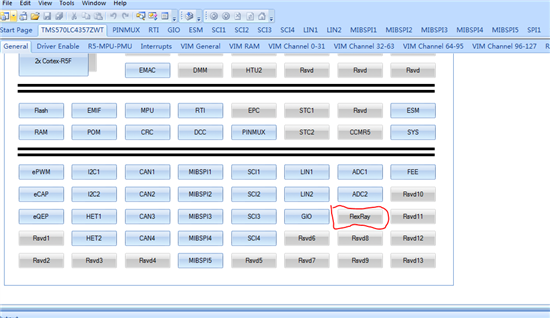
这种情况下是不是不能通过此软件来配置FlexRay功能的使用?如果不能的话请问TI是否有FlexRay功能的例程?如果这个软件不能配置,是不是代表这个芯片没有FlexRay功能?
↧
RM46L852
本人使用RM46L852芯片,仿真状态MDIOInit(hdkif->mdio_base,MDIO_FREQ_INPUT,MDIO_FREQ_OUTPUT)初始化完成后,MDIO输出口就不断发送数据,程序打了断点,MDIO口还是不受控制的发送数据,有哪位知道是什么情况?
↧